


TOSHIBA Bipolar Digital Integrated Circuit Silicon Monolithic
ULN2803APG,ULN2803AFWG,ULN2804APG,ULN2804AFWG (Manufactured by Toshiba Malaysia)
8ch Darlington Sink Driver
The ULN2803APG / AFWG Series are high−voltage, high−current darlington drivers comprised of eight NPN darlington pairs.
All units feature integral clamp diodes for switching inductive loads.
Applications include relay, hammer, lamp and display (LED)
drivers.
The suffix (G) appended to the part number represents a Lead
(Pb)-Free product.
Features
z Output current (single output)
500 mA (Max.)
z High sustaining voltage output
50 V (Min.)
z Output clamp diodes
z Inputs compatible with various types of logic.
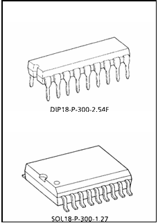
z Package Type−APG : DIP−18pin
z Package Type−AFWG : SOL−18pin
ULN2803APG ULN2804APG
ULN2803AFWG ULN2804AFWG
Weight
DIP18−P−300−2.54F: 1.478 g (Typ.) SOL18−P−300−1.27 : 0.48 g (Typ.)
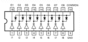
Pin Connection (top view)
|
Type |
Input Base Resistor |
Designation |
|
ULN2803APG / AFWG |
2.7 kΩ |
TTL, 5 V CMOS |
|
ULN2804APG / AFWG |
10.5 kΩ |
6~15 V PMOS, CMOS |
Schematics (each driver)
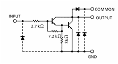
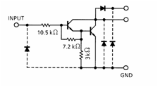 ULN2803APG / AFWG ULN2804APG / AFWG
Note: The input and output parasitic diodes cannot be used as clamp diodes.
Absolute Maximum Ratings (Ta = 25°„C)
|
Characteristic |
Symbol |
Rating |
Unit |
|
|
Output sustaining voltage |
VCE (SUS) |
−0.5~50 |
V |
|
|
Output current |
IOUT |
500 |
mA / ch |
|
|
Input voltage |
VIN |
−0.5~30 |
V |
|
|
Clamp diode reverse voltage |
VR |
50 |
V |
|
|
Clamp diode forward current |
IF |
500 |
mA |
|
|
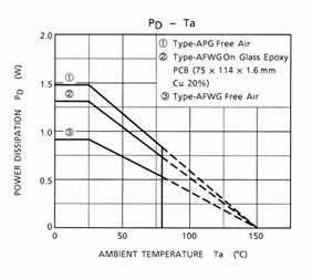
Power dissipation |
APG |
PD |
1.47 |
W |
|
AFWG |
0.92 / 1.31 (Note) |
|||
|
Operating temperature |
Topr |
−40~85 |
°„C |
|
|
Storage temperature |
Tstg |
−55~150 |
°„C |
|
Note: On Glass Epoxy PCB (75 °¡ 114 °¡ 1.6 mm Cu 20%)
Recommended Operating Conditions (Ta = −40~85°„C)
|
Characteristic |
Symbol |
Test Condition |
Min |
Typ. |
Max |
Unit |
|
|
Output sustaining voltage |
VCE (SUS) |
|
0 |
®D |
50 |
V |
|
|
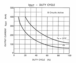
Output current |
APG |
IOUT |
Tpw = 25 ms, Duty = 10%, 8 Circuits |
0 |
®D |
347 |
mA / ch |
|
Tpw = 25 ms, Duty = 50%, 8 Circuits |
0 |
®D |
123 |
||||
|
AFWG |
Tpw = 25 ms, Duty = 10%, 8 Circuits |
0 |
®D |
268 |
|||
|
Tpw = 25 ms, Duty = 50%, 8 Circuits |
0 |
®D |
90 |
||||
|
Input voltage |
VIN |
|
0 |
®D |
30 |
V |
|
|
Input voltage (Output on) |
ULN2803A |
VIN (ON) |
|
3.5 |
®D |
30 |
V |
|
ULN2804A |
|
8 |
®D |
30 |
|||
|
Clamp diode reverse voltage |
VR |
|
®D |
®D |
50 |
V |
|
|
Clamp diode forward current |
IF |
|
®D |
®D |
400 |
mA |
|
|
Power dissipation |
APG |
PD |
Ta = 85°„C |
®D |
®D |
0.76 |
W |
|
AFWG |
Ta = 85°„C (Note) |
®D |
®D |
0.48 |
|||
Note: On Glass Epoxy PCB (75 °¡ 114 °¡ 1.6 mm Cu 20%)
Electrical Characteristics (Ta = 25°„C)
|
Characteristic |
Symbol |
Test Cir− Cuit |
Test Condition |
Min |
Typ. |
Max |
Unit |
||
|
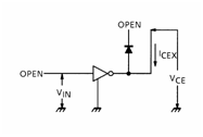
Output leakage current |
ICEX |
1 |
VCE = 50 V |
Ta = 25°„C |
®D |
®D |
50 |
µA |
|
|
VCE = 50 V |
Ta = 85°„C |
®D |
®D |
100 |
|||||
|
|
ULN2804A |
VCE = 50 V |
VIN = 1 V |
®D |
®D |
500 |
|||
|
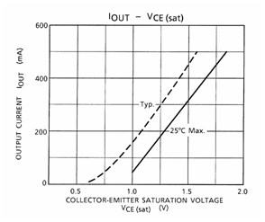
Collector−emitter saturation voltage |
VCE (sat) |
2 |
IOUT = 350 mA, IIN = 500 µA |
®D |
1.3 |
1.6 |
V |
||
|
IOUT = 200 mA, IIN = 350 µA |
®D |
1.1 |
1.3 |
||||||
|
IOUT = 100 mA, IIN = 250 µA |
®D |
0.9 |
1.1 |
||||||
|
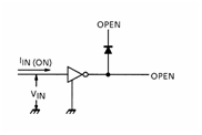
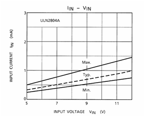
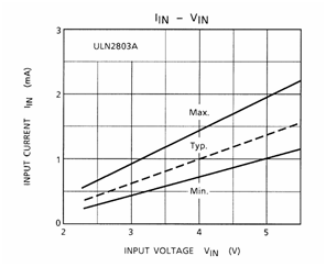
Input current |
ULN2803A |
IIN (ON) |
2 |
VIN = 3.85 V |
®D |
0.93 |
1.35 |
mA |
|
|
ULN2804A |
VIN = 5 V |
®D |
0.35 |
0.5 |
|||||
|
VIN = 12 V |
®D |
1.0 |
1.45 |
||||||
|
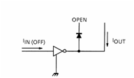
|
IIN (OFF) |
4 |
IOUT = 500 µA, Ta = 85°„C |
50 |
65 |
®D |
µA |
||
|
Input voltage (Output on) |
ULN2803A |
VIN (ON) |
5 |
VCE = 2 V, IOUT = 200 mA |
®D |
®D |
2.4 |
V |
|
|
VCE = 2 V, IOUT = 250 mA |
®D |
®D |
2.7 |
||||||
|
VCE = 2 V, IOUT = 300 mA |
®D |
®D |
3.0 |
||||||
|
ULN2804A |
VCE = 2 V, IOUT = 125 mA |
®D |
®D |
5.0 |
|||||
|
VCE = 2 V, IOUT = 200 mA |
®D |
®D |
6.0 |
||||||
|
VCE = 2 V, IOUT = 275 mA |
®D |
®D |
7.0 |
||||||
|
VCE = 2 V, IOUT = 350 mA |
®D |
®D |
8.0 |
||||||
|
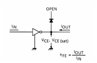
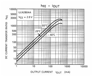
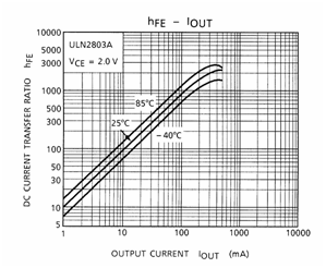
DC current transfer ratio |
hFE |
2 |
VCE = 2 V, IOUT = 350 mA |
1000 |
®D |
®D |
|
||
|
Clamp diode reverse current |
IR |
6 |
Ta = 25°„C (Note) |
®D |
®D |
50 |
µA |
||
|
Ta = 85°„C (Note) |
®D |
®D |
100 |
||||||
|
Clamp diode forward voltage |
VF |
7 |
IF = 350 mA |
®D |
®D |
2.0 |
V |
||
|
Input capacitance |
CIN |
®D |
|
®D |
15 |
®D |
pF |
||
|
Turn−on delay |
tON |
8 |
RL = 125 Ω, VOUT = 50 V |
®D |
0.1 |
®D |
µs |
||
|
Turn−off delay |
tOFF |
RL = 125 Ω, VOUT = 50 V |
®D |
0.2 |
®D |
||||
Note: VR = VR MAX.
Test Circuit
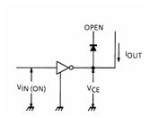
 1. ICEX 2. VCE (sat), hFE 3. IIN (ON)
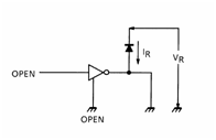 4. IIN (OFF) 5. VIN (ON) 6. IR
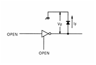 7. VF
7. VF
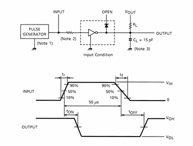 8. tON, tOFF
Note 1: Pulse Width 50 µs, Duty Cycle 10%
Output Impedance 50 Ω, tr °Ð 5 ns, tf °Ð 10 ns
Note 2: See below.
Input Condition
|
Type Number |
R1 |
VIH |
|
ULN2803A |
0Ω |
3 V |
|
ULN2804A |
0Ω |
8 V |
Note 3: CL includes probe and jig capacitance
Precautions for Using
This IC does not integrate protection circuits such as overcurrent and overvoltage protectors.
Thus, if excess current or voltage is applied to the IC, the IC may be damaged. Please design the IC so that excess current or voltage will not be applied to the IC.
Utmost care is necessary in the design of the output line, COMMON and GND line since IC may be destroyed due to short−circuit between outputs, air contamination fault, or fault by improper grounding.
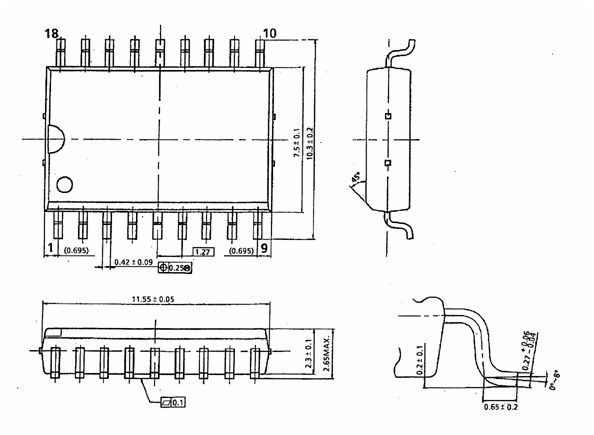
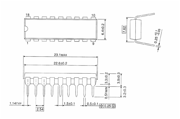 Package Dimensions
DIP18−P−300−2.54F Unit: mm
Weight: 1.478 g (Typ.)
Package Dimensions
 SOL18−P−300−1.27 Unit: mm
Weight: 0.48 g (Typ.)
Notes on Contents
1. Schematics
The schematics may be simplified or some parts of them may be omitted for explanatory purposes.
2. Absolute Maximum Ratings
The absolute maximum ratings of a semiconductor device are a set of specified parameter values that must not be exceeded during operation, even for an instant.
If any of these ratings are exceeded during operation, the electrical characteristics of the device may be irreparably altered and the reliability and lifetime of the device can no longer be guaranteed.
Moreover, any exceeding of the ratings during operation may cause breakdown, damage and/or degradation in other equipment. Applications using the device should be designed so that no absolute maximum rating will ever be exceeded under any operating conditions.
Before using, creating and/or producing designs, refer to and comply with the precautions and conditions set forth in this document.
3. Recommended Operating Conditions
The values of the conditions are applied within the range of the operating temperature and not guaranteed.
4. AC Characteristics
AC characteristics that mean turn-on and turn-off time are targeted design values and not guaranteed.
5. Application Circuits
The application circuits shown in this document are provided for reference purposes only. Thorough evaluation is required, especially in the phase of mass production design.
In furnishing these examples of application circuits, Toshiba does not grant the use of any industrial property rights.
6. Graphics Characteristics
Graphics characteristics are reference ones and not guaranteed.
Handling of the IC
Ensure that the product is installed correctly to prevent breakdown, damage and/or degradation in the product or equipment.
Contact Person: liao
Skype: Aunytor
Email: 2885745253@qq.com