


LTC6416 - 2GHz Low Noise Differential 16-Bit ADC Buffer
°§ 2GHz ®C3dB Small Signal Bandwidth
°§ 300MHz °¿0.1dB Bandwidth
°§ 1.8nV/°ÃHz Output Noise
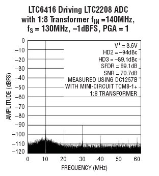
°§ 46.25dBm Equivalent OIP3 at 140MHz
°§ 40.25dBm Equivalent OIP3 Up to 300MHz
°§ ®C81dBc/®C72dBc HD2/HD3 at 140MHz, 2VP-P Out
°§ ®C84.5dBc IM3 at 140MHz, 2VP-P Out Composite
°§ ®C74dBc/®C67.5dBc HD2/HD3 at 300MHz, 2VP-P Out
°§ ®C72.5dBc IM3 at 300MHz, 2VP-P Out Composite
°§ Programmable High Speed, Fast Recovery Output Clamping
°§ DC-Coupled Signal Path
°§ Operates on Single 2.7V to 3.9V Supply
°§ Low Power: 150mW on 3.6V
°§
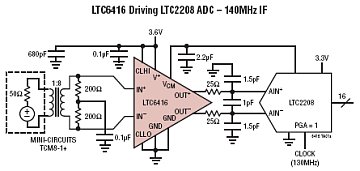
Typical Application
Description
The LTC6416 is a differential unity gain buffer designed to drive 16-bit ADCs with extremely low output noise and excellent linearity beyond 300MHz. Differential input impedance is 12k¶∏, allowing 1:4 and 1:8 transformers to be used at the input to achieve additional system gain.
With no external biasing or gain setting components and a flow-through pinout, the LTC6416 is very easy to use. It can be DC-coupled and has a common mode output offset of ®C40mV. If the input signals are AC-coupled, the LTC6416 input pins are internally biased to provide an output common mode voltage that is set by the voltage on the VCM pin.
In addition the LTC6416 has high speed, fast recovery clamping circuitry to limit output signal swing. Both the high and low clamp voltages are internally biased to allow maximum output swing but are also user programmable via the CLLO and CLHI pins.
Supply current is nominally 42mA and the LTC6416 operates on supply voltages ranging from 2.7V to 3.9V.
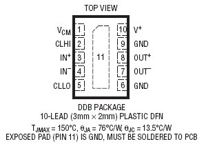
The LTC6416 is packaged in a 10-lead
Packaging
DFN-10
FROM: Company Name: Aunytor Electronic (HK) Co.,Ltd
Contact Person: liao
Skype: Aunytor
Email: 2885745253@qq.com