


LTC4307 - Low Offset Hot Swappable 2-Wire Bus Buffer with Stuck Bus Recovery
°§ Bidirectional Buffer with Stuck Bus Recovery
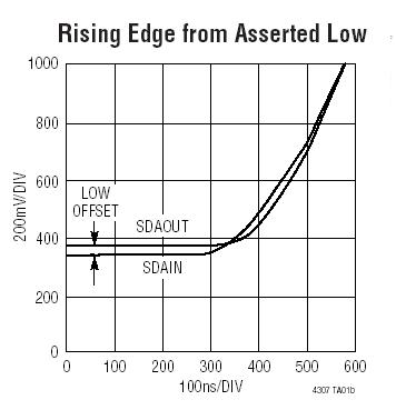
°§ 60mV Buffer Offset Independent of Load
°§ 30ms Stuck Bus Timeout
°§ Compatible with Non-Compliant VOL I
°§ Prevents SDA and SCL Corruption During Live Board Insertion and Removal from Backplane
°§ °¿5kV Human Body Model ESD Protection
°§ Isolates Input SDA and SCL Line from Output
°§ Compatible with I
°§ READY Open-Drain Output
°§ 1V Precharge on All SDA and SCL Lines
°§ High Impedance SDA, SCL Pins for VCC = 0V
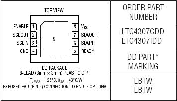
°§ Small 8-Lead (
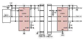
Typical Application
Description
The LTC4307 hot swappable, 2-wire bus buffer allows I/O card insertion into a live backplane without corruption of the data and clock busses. The LTC4307 provides bidirectional buffering, keeping the backplane and card capacitances isolated. Low offset and high VOL tolerance allows multiple devices to be cascaded on the clock and data busses. If SDAOUT or SCLOUT are low for 30ms, the LTC4307 will automatically break the bus connection. At this time the LTC4307 automatically generates up to 16 clock pulses on SCLOUT in an attempt to free the bus. A connection will resume if the stuck bus is cleared.
During insertion, the SDA and SCL lines are pre-charged to 1V to minimize bus disturbances. When driven high, the ENABLE input allows the LTC4307 to connect after a stop bit or bus idle. Driving ENABLE low breaks the connection between SDAIN and SDAOUT, SCLIN and SCLOUT. READY is an open-drain output which indicates that the backplane and card sides are connected.
Packaging
DFN-8, MSOP-8

.
.FROM: Company Name: Aunytor Electronic (HK) Co.,Ltd
Contact Person: liao
Skype: Aunytor
Email: 2885745253@qq.com