


DESCRIPTION
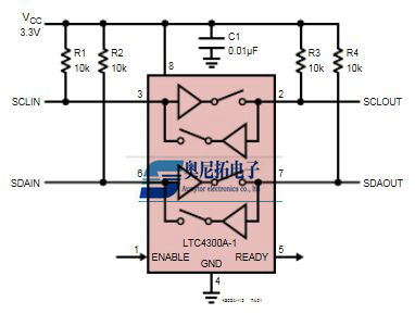
The LTC4300A series hot swappable 2-wire bus buffers
allow I/O card insertion into a live backplane without
corruption of the data and clock busses. When the con-
nection is made, the LTC4300A-1/LTC4300A-2 provide
bidirectional buffering, keeping the backplane and card
capacitances isolated. Rise-time accelerator circuitry*
allows the use of weaker DC pull-up currents while still
meeting rise-time requirements. During insertion, the
SDA and SCL lines are precharged to 1V to minimize bus
disturbances.
The LTC4300A-1 incorporates a CMOS threshold digital
ENABLE input pin, which forces the part into a low current
mode when driven to ground and sets normal operation when
driven to VCC. It also includes an open drain READY output
pin, which indicates that the backplane and card sides are
connected together. The LTC4300A-2 replaces the ENABLE
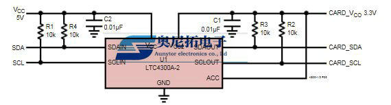
pin with a dedicated supply voltage pin, VCC2, for the card
side, providing level shifting between 3.3V and 5V systems.
Both the backplane and card may be powered with supply
voltages ranging from 2.7V to 5.5V, with no contraints on
which supply voltage is higher. The LTC4300A-2 also re-
places the READY pin with a digital CMOS input pin, ACC,
which enables and disables the rise-time accelerator currents.
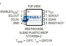
The LTC4300A is available in a small 8-pin MSOP package.
FEATURES
Bidirectional Buffer for SDA and SCL Lines
Increases Fanout
Prevents SDA and SCL Corruption During Live
Board Insertion and Removal from Backplane
Isolates Input SDA and SCL Lines from Output
Compatible with I2C, I 2 C Fast Mode and SMBus
Standards (Up to 400kHz Operation)
Small MSOP 8-Pin Package
Low ICC Chip Disable: <1µA (LTC4300A-1)
READY Open Drain Output (LTC4300A-1)
1V Precharge on all SDA and SCL Lines
Supports Clock Stretching, Arbitration and
Synchronization
5V to 3.3V Level Translation (LTC4300A-2)
High Impedance SDA, SCL Pins for VCC = 0V
APPLICATIONS
Hot Board Insertion
Servers
Capacitance Buffer/Bus Extender
Desktop Computer
TYPICAL APPLICATION
Input–Output Connection
MSS PACKAGE
TYPICAL APPLICATIONS
System with Disparate VCC Voltages
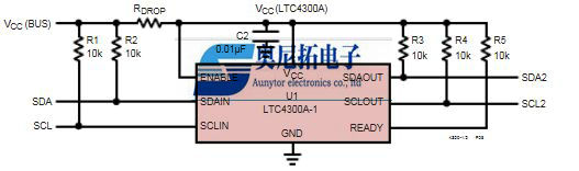
5V to 3.3V Level Translator
P/N Package
LTC4300A-2CMS8 MSOP8
LTC4300A-2IMS8 MSOP8
LTC4300A-1CMS8 MSOP8
LTC4300A-1IMS8 MSOP8
FROM: Company Name: Aunytor Electronic (HK) Co.,Ltd
Contact Person: liao
Skype: Aunytor
Email: 2885745253@qq.com