


Description
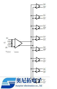
The NB7L1008M is a high performance differential
1:8 Clock/Data fanout buffer. The NB7L1008M produces
eight identical output copies of Clock or Data
operating up to 6 GHz or 10.7 Gb/s, respectively. As
such,the NB7L1008M is ideal for SONET,GigE,Fiber Channel,
Backplane and other Clock/Data distribution applications.
The differential inputs incorporate internal 50W termination
resistors that are accessed through the VT pin. This
feature allows the NB7L1008M to accept various logic standards,
such as LVPECL,CML,LVDS,LVCMOS or LVTTL logic levels. The V REFAC
reference output can be used to rebias capacitor−coupled
differential or single−ended inputsignals. The 1:8 fanout design
was optimized for low output skew applications. The NB7L1008M
is a member of the GigaComm™family of high performance clock products.
Features
Input Data Rate > 12 Gb/s Typical
Data Dependent Jitter < 20 ps
Maximum Input Clock Frequency > 8 GHz Typical
andom Clock Jitter < 0.8 ps RMS
Low Skew 1:8 CML Outputs, < 25ps max
Multi−Level Inputs, accepts LVPECL, CML, LVDS
160 ps Typical Propagation Delay
45 ps Typical Rise and Fall Times
Differential CML Outputs, 400 mV Peak−to−Peak, Typical
Operating Range: V CC = 2.375V to 3.6V, GND = 0V
Internal Input Termination Resistors, 50W
V REFAC Reference Output
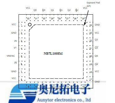
QFN−32 Package, 5mm x 5mm
−40°Ê to +85°Ê Ambient Operating Temperature
These are Pb−Free Devices
SIMPLIFIED LOGIC DIAGRAM
32−Lead QFN Pinout(Top View)
P/N Package
NB7L1008MMNG QFN32
NB7L1008MMNR4G QFN32
FROM: Company Name: Aunytor Electronic (HK) Co.,Ltd
Contact Person: liao
Skype: Aunytor
Email: 2885745253@qq.com