


Description
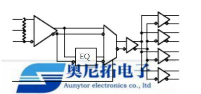
The NB6HQ14M is a high performance differential 1:4
CML fanout buffer with a selectable Equalizer receiver.
When placed in series with a Clock /Data path operating
up to 5 GHz or 6.5 Gb/s, respectively,the NB6HQ14M inputs
will compensate the degraded signal transmitted across
a FR4 PCB backplane or cable interconnect and output four
identical CML copies of the input signal. Therefore,
the serial data rate is increased by reducing Inter−Symbol
Interference (ISI) caused by losses in copper interconnect
or long cables.The EQualizer ENable pin (EQEN) allows the
IN/IN inputs to either flow through or bypass the Equalizer
section. Control of the Equalizer function is realized by
setting EQEN;When EQEN is set Low, the IN/IN inputs bypass the
Equalizer.When EQEN is set High,the IN/IN inputs flow through the
Equalizer.The default state at start−up is LOW. As such,NB6HQ14M
is ideal for SONET, GigE, Fiber Channel, Backplane and other
Clock/Data distribution applications.
The differential inputs incorporate internal 50W termination
resistors that are accessed through the VT pin. This feature allows
the NB6HQ14M to accept various logic level standards, such as LVPECL,
CML or LVDS.The outputs have the flexibility of being powered by
either a 2.5V or 1.8V supply. The 1:4 fanout design was optimized
for low output skew applications.
The NB6HQ14M is a member of the ECLinPS MAX™ family of
high performance clock products.
Features
Input Data Rate > 6.Gb/s
Input Clock Frequency > 5GHz
170ps Typical Propagation Delay
35ps Typical Rise and Fall Times
< 15ps Output Skew
< 0.8ps RMS Clock Jitter
< 10ps pp of Data Dependent Jitter
Differential CML Outputs, 400 mV Peak−to−Peak, Typical
Selectable Input Equalization
Operating Range: VCC= 2.375V to 2.625V, V CCO= 1.71V to
2.625V
Internal Input Termination Resistors, 50W
−40°Ê to +85°Ê Ambient Operating Temperature
These are Pb−Free Devices
SIMPLIFIED BLOCK DIAGRAM
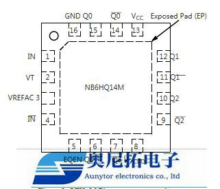
PIN DESCRIPTION
P/N Package
NB6HQ14MMNG QFN-16
NB6HQ14MMNHTBG QFN-16
NB6HQ14MMNTXG QFN-16