

| 型號 | 品牌 | 批號 | 數量 | 封裝 | 備注 |
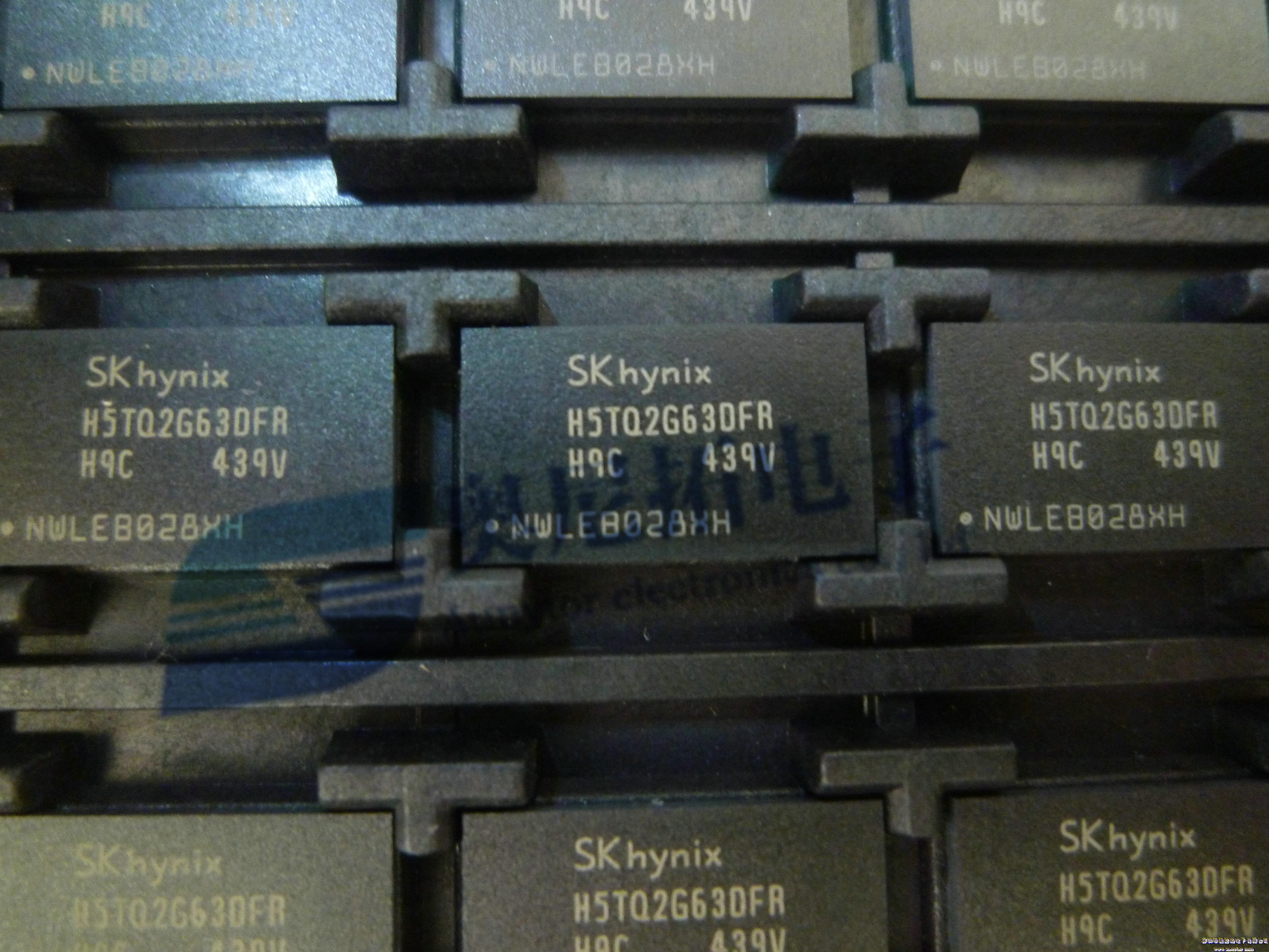
| H5TQ2G63DFR | HYNIX | 22+ | 5000000 | BGA | Original 全新原裝 |
H5TQ2G63DFR![]() pdf規格書
pdf規格書

H5TQ2G63DFRDescription
While all addresses and
control inputs are latched on the rising edges of the CK (falling edges of the CK), Data, Data strobes and
Write data masks inputs are sampled on both rising and falling edges of it. The data paths are internally
pipelined and 8-bit prefetched to achieve very high bandwidth.
H5TQ2G63DFRFEATURES
• This product in compliance with the RoHS directive.
• VDD=VDDQ=1.5V +/- 0.075V
• Fully differential clock inputs (CK, CK) operation
• Differential Data Strobe (DQS, DQS)
• On chip DLL align DQ, DQS and DQS transition with CK
transition
• DM masks write data-in at the both rising and falling
edges of the data strobe
• All addresses and control inputs except data,
data strobes and data masks latched on the
rising edges of the clock
• Programmable CAS latency 5, 6, 7, 8, 9, 10, 11, 12, 13
and 14 supported
• Programmable additive latency 0, CL-1, and CL-2
supported
• Programmable CAS Write latency (CWL) = 5, 6, 7, 8
• Programmable burst length 4/8 with both nibble
sequential and interleave mode
• BL switch on the fly
• 8banks
• Average Refresh Cycle (Tcase 0 oC~ 95 oC)
- 7.8 µs at 0oC ~ 85 oC
- 3.9 µs at 85oC ~ 95 oC
Commercial Temperature( 0oC ~ 85 oC)
Industrial Temperature( -40oC ~ 95 oC)
• Auto Self Refresh supported
• JEDEC standard 78ball FBGA(x8), 96ball FBGA(x16)
• Driver strength selected by EMRS
• Dynamic On Die Termination supported
• Asynchronous RESET pin supported
• ZQ calibration supported
• TDQS (Termination Data Strobe) supported (x8 only)
• Write Levelization supported
• 8 bit pre-fetch
IDD and IDDQ Specification Parameters and Test Conditions
IDD and IDDQ Measurement Conditions
In this chapter, IDD and IDDQ measurement conditions such as test load and patterns are defined. Figure
1. shows the setup and test load for IDD and IDDQ measurements.
• IDD currents (such as IDD0, IDD1, IDD2N, IDD2NT, IDD2P0, IDD2P1, IDD2Q, IDD3N, IDD3P, IDD4R,
IDD4W, IDD5B, IDD6, IDD6ET, IDD6TC and IDD7) are measured as time-averaged currents with all
VDD balls of the DDR3 SDRAM under test tied together. Any IDDQ current is not included in IDD cur-
rents.
• IDDQ currents (such as IDDQ2NT and IDDQ4R) are measured as time-averaged currents with all
VDDQ balls of the DDR3 SDRAM under test tied together. Any IDD current is not included in IDDQ cur-
rents.
Attention: IDDQ values cannot be directly used to calculate IO power of the DDR3 SDRAM. They can
be used to support correlation of simulated IO power to actual IO power as outlined in Figure 2. In
DRAM module application, IDDQ cannot be measured separately since VDD and VDDQ are using one
merged-power layer in Module PCB.
For IDD and IDDQ measurements, the following definitions apply:
• ”0” and “LOW” is defined as VIN <= V ILAC(max).
• ”1” and “HIGH” is defined as VIN >= V IHAC(max).
• “MID_LEVEL” is defined as inputs are VREF = VDD/2.
• Timing used for IDD and IDDQ Measurement-Loop Patterns are provided in Table 1.
• Basic IDD and IDDQ Measurement Conditions are described in Table 2.
• Detailed IDD and IDDQ Measurement-Loop Patterns are described in Table 3 through Table 10.
• IDD Measurements are done after properly initializing the DDR3 SDRAM. This includes but is not lim-
ited to setting
RON = RZQ/7 (34 Ohm in MR1);
Qoff = 0 B (Output Buffer enabled in MR1);
RTT_Nom = RZQ/6 (40 Ohm in MR1);
RTT_Wr = RZQ/2 (120 Ohm in MR2);
TDQS Feature disabled in MR1
• Attention: The IDD and IDDQ Measurement-Loop Patterns need to be executed at least one time
before actual IDD or IDDQ measurement is started.
• Define D = {CS, RAS, CAS, WE}:= {HIGH, LOW, LOW, LOW}
• Define D = {CS, RAS, CAS, WE}:= {HIGH, HIGH, HIGH, HIGH}
H5TQ2G63DFR描述
盡管所有地址和控制輸入的邊緣上升的CK(CK)的邊緣下降,數據,數據用閃光燈和面具寫入數據輸入采樣在上升和下降的邊緣。數據路徑內部流水線和8位預取的實現非常高的帶寬。
H5TQ2G63DFR特性
•VDD = VDDQ = 1.5 v + / - 0.075 v
•完全微分時鐘輸入(CK、CK)操作
•微分數據(dq,dq)
•在芯片DLL對齊DQ、DQ和DQ與CK過渡轉型
•DM面具寫數據輸入的數據選通脈沖的上升和下降的邊緣
•所有地址和控制輸入,除了數據,數據用閃光燈和數據掩蓋了鎖定在時鐘的上升的邊緣
•可編程CAS延遲5、6、7、8、9、10、11、12、13和14支持
•可編程添加劑延遲0、CL-1 CL-2支持
•可編程脈沖時間4/8咬順序和交錯模式
•提單開關
•平均刷新周期(Tcase 0攝氏度~ 95攝氏度)
- µs at - 7.8 0oC ~ 85 oC
- 3.9µs在85度~ 95度
商業溫度(0攝氏度~ 85攝氏度)
工業溫度(-40度~ 95度)
•汽車自我更新的支持
•JEDEC標準78球FBGA(x8 -),96球FBGA(x16)
•驅動力量選擇電子病歷
•動態模終止支持
•異步復位銷支持
•ZQ校準支持
•TDQS(終止數據選通)支持(×8只)
•寫Levelization支持
•8位預取
IDD和IDDQ規范參數
IDD和IDDQ測試條件和測試條件
•IDD電流(例如IDD0、IDD1 IDD2N,IDD2NT,IDD2P0,IDD2P1,IDD2Q,IDD3N,IDD3P,IDD4R,IDD4W,IDD5B,IDD6,IDD6ET,IDD6TC和IDD7)測量是時間上的電流與所有VDD球DDR3 SDRAM測試下綁在一起。不包括任何IDDQ當前IDD。
•IDDQ電流(例如IDDQ2NT和IDDQ4R)測量上的電流與所有VDDQ球DDR3 SDRAM測試下綁在一起。不包括任何IDD當前IDDQ壞蛋——租金。
注意:
IDDQ值不能直接用來計算IO DDR3 SDRAM的力量。他們可以用來支持相關的模擬輸入輸出功率實際輸入輸出功率如圖2中列出。分別在DRAM模塊應用程序中,IDDQ無法衡量自VDD VDDQ使用模塊PCB merged-power層之一。
對于IDD和IDDQ測試,以下定義適用:
•“0”和“低”的定義是VIN < = V ILAC(max)。
•“1”和“高”被定義為VIN > = V IHAC(max)。
•“MID_LEVEL”被定義為輸入VREF = VDD / 2。
•時間用于IDD和IDDQ Measurement-Loop模式是表1中提供。
•基本IDD和IDDQ測試條件如表2中所描述的。
•詳細IDD和IDDQ Measurement-Loop模式是描述在表3表10。
•IDD測量正確初始化DDR3 SDRAM后完成。這包括但不僅lim -報道設置
•注意:IDD和IDDQ Measurement-Loop模式需要執行至少一個實際IDD或IDDQ測試開始時間。
•定義D = { CS,RAS,中科院,我們}:= {高、低、低、低}
•定義D = { CS,RAS,中科院,我們}:= {高,高,高,高}
FROM: Company Name: Aunytor Electronic (HK) Co.,Ltd
Contact Person: liao
Skype: Aunytor
Email: 2885745253@qq.com
原裝進口,現貨庫存,歡迎來電咨詢:聯系方式如下
名稱: 深圳奧尼拓電子有限公司
地址: 深圳市福田區中航路都會軒3707-3708室
電話: 19539046113
QQ : 2885745253
企業郵箱:2885745253@qq.com
聯系人: 廖麗玲
來源:深圳市奧尼拓電子有限公司
網址:http://www.aunytorchips.com/