

| 型號 | 品牌 | 批號 | 數量 | 封裝 | 備注 |
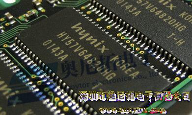
| HY57V64820HG | HYNIX | 22+ | 5000000 | TSOP | Original 全新原裝 |
HY57V64820HG![]() pdf規格書
pdf規格書

HY57V64820HGDESCRIPTION
The Hynix HY57V64820HG is a 67,108,864-bit CMOS Synchronous DRAM, ideally suited for the main memory applications which
require large memory density and high bandwidth. HY57V64820HG is organized as 4banks of 2,097,152x8.
Programmable options include the length of pipeline (Read latency of 2 or 3), the number of consecutive read or write cycles initiated by
a single control command (Burst length of 1,2,4,8 or Full page), and the burst count sequence(sequential or interleave). A burst of read
or write cycles in progress can be terminated by a burst terminate command or can be interrupted and replaced by a new burst read or
write command on any cycle. (This pipelined design is not restricted by a `2N` rule.)
HY57V64820HGFEATURES
• Single 3.3±0.3V power supply
• All device pins are compatible with LVTTL interface
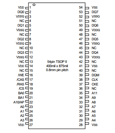
• JEDEC standard 400mil 54pin TSOP-II with 0.8mm of pin pitch
• Data mask function by DQM
• Internal four banks operation
• Auto refresh and self refresh
• 4096 refresh cycles / 64ms
• Programmable Burst Length and Burst Type
- 1, 2, 4, 8 or Full page for Sequential Burst
- 1, 2, 4 or 8 for Interleave Burst
• Programmable CAS Latency ; 2, 3 Clocks
HY57V64820HG描述
HY57V64820HG是67108864位CMOS同步DRAM,適合主內存的應
用程序需要大內存密度和高帶寬。HY57V64820HG被組織為
4 2097152×8的銀行。
可編程選項包括管道的長度(讀延遲2或3),連續讀或寫的循
環次數由一個單一的控制命令(區間長度的1、2、4、8或整頁),
和破裂計數序列(序列或交錯)。一陣讀或寫周期進展可以終止
破裂終止命令或可以被打斷,取而代之的是一個新的破裂讀或
寫命令在任何周期。(這個流水線設計是不受限制的“2 n”規則。)
HY57V64820HG特性
•單3.3±0.3 v電源
•所有設備銷與LVTTL接口是兼容的
•JEDEC標準400毫升54銷TSOP-II針距的0.8毫米
•DQM數據屏蔽功能
•內部四家銀行操作
•自動刷新和自我更新
•4096刷新周期/ 64 ms
•可編程破裂長度和破裂類型
- 1,2,4,8或整頁順序
- 1,2、4或8交錯破裂
•可編程CAS延遲;2、3時鐘
HY57V64820HGPIN CONFIGURATION
HY57V64820HG引線結構
原裝進口,現貨庫存,歡迎來電咨詢:聯系方式如下
名稱: 深圳奧尼拓電子有限公司
地址: 深圳市福田區中航路都會軒3707-3708室
電話: 19539046113
QQ : 2885745253
企業郵箱:2885745253@qq.com
聯系人: 廖麗玲
來源:深圳市奧尼拓電子有限公司
網址:http://www.aunytorchips.com/