Hot Search:apw 2030 4832 APW   English       繁體中文
|
|
|
|
|
|
|
|
|
About US
Quick Search Stock A B C D E F G H I J K L M N O P Q R S T U V W X Y Z 0 1 2 3 4 5 6 7 8 9
New stock
Download
MSP430F5172IRSBR TI
RF430F5144CIRKVRQ1 TI
TQP7M9102 QORVO
HY57V64820HG HYNIX
H5TQ2G63DFR HYNIX
XC2C512-10FT256I XILINX
XC2C512-10FG324I XILINX
XC2C512 XILINX
XC2C384-7TQG144C XILINX
XC2C384-7FGG324C XILINX
XC2C384-10TQG144I XILINX
XC2C384-10TQG144C XILINX
XC2C384-10TQ144I XILINX
XC2C384-10PQG208I XILINX
XC2C384-10PQG208C XILINX
XC2C384-10PQ208I XILINX
Contact

Total Stock:118849
Update:2025-08-13

Tel:+86 19539046113
Tel:+86 0755-82558684
Fax:+86 0755-82530730
Mail:carrot@aunytorchips.com .


News & Events Path:Home > MC74VHC1GT66: Single Supply Analog Switch

MC74VHC1GT66: Single Supply Analog Switch


From:www.aunytor.com | Date:2024-04-12

Product Description :

The MC74VHC1GT66 is an advanced high speed CMOS bilateral analog switch fabricated with silicon gate CMOS technology. It achieves high speed propagation delays and low ON resistances while maintaining CMOS low power dissipation. This bilateral switch controls analog and digital voltages that may vary across the full power-supply range (from VCC to GND).

The MC74VHC1GT66 is compatible in function to a single gate of the very High Speed CMOS MC74VHCT4066. The device has been designed so that the ON resistances (RON) are much lower and more linear over input voltage than RON of the metal-gate CMOS or High Speed CMOS analog switches.

The ON/OFF Control input is compatible with TTL-type input thresholds allowing the device to be used as a logic-level translator from 3.0V CMOS logic to 5.0V CMOS logic or from 1.8V CMOS logic to3.0V CMOS logic while operating at the high-voltage power supply. The input protection circuitry on this device allows overvoltage tolerance onthe input, which provides protection when voltages of up to 7V are applied, regardless of the supply voltage. This allows the MC74VHC1GT66 to be used to interface 5V circuits to 3V circuits.

Features :

  • High Speed: tPD = 20 ns (Typ) at VCC = 5 V
  • Low Power Dissipation: ICC = 1µA (Max) at TA = 25°C
  • Diode Protection Provided on Inputs and Outputs
  • Improved Linearity and Lower ON Resistance over Input Voltage
  • On/Off Control Input Has OVT
  • Chip Complexity: FETs = 11; Equivalent Gates = 3
  • Pb-Free Packages are Available

Applications :

  • Cell Phones
  • Wireless Consumer Devices
  • Portable Computing
  • Low Voltage Data Acquisition
  • Audio and Video Signal Routing

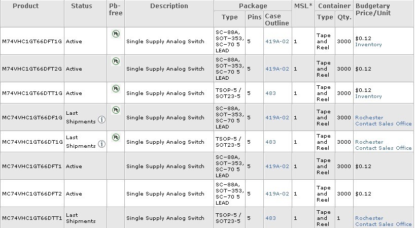
    Availability and Samples:


    Functional Block Diagram :


    FROM: Company Name: Aunytor Electronic (HK) Co.,Ltd
                Contact Person: liao
                Skype: Aunytor
                Email: 2885745253@qq.com

  • Pre:ADT7461: +/-1C TDM Extended Temp Range I.C.
    Next:MC33340: Battery Fast Charge Controller
     
    Home | About | Stock | News & Events | Download | Online order | Contact| Bank account
    Copyright @ 2009 - 2024 Aunytor. All Rights Reserved ICP备案/许可证号:粤ICP备17017679号-4