


DESCRIPTION
The 74LV14 is a low-voltage Si-gate CMOS
device and is pin and function compatible
with 74HC/HCT14.The 74LV14 provides six
inverting buffers with Schmitt-trigger
action. It is capable of transforming
slowly changing input signals into sharply
defined, jitter-free output signals.
FEATURES
Wide operating voltage: 1.0 to 5.5 V
Optimized for Low Voltage applications: 1.0 to 3.6
Accepts TTL input levels between VCC= 2.7 V and VCC= 3.6 V
Typical VOLP(output ground bounce) < 0.8 V at VCC= 3.3 V,
Tamb = 25℃
Typical VOHV(output Vundershoot) > 2 V at VCC= 3.3 V,
Tamb = 25℃
Output capability: standard
ICC category: SSI
APPLICATIONS
Wave and pulse shapers for highly noisy environments
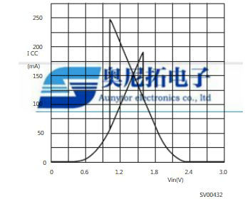
TRANSFER CHARACTERISTIC WAVEFORMS
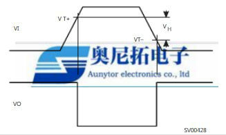
Transfer characteristic
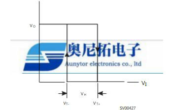
Definition of V T),VT-and VH;
where V T+and V T-are between limits of 20% and 70%
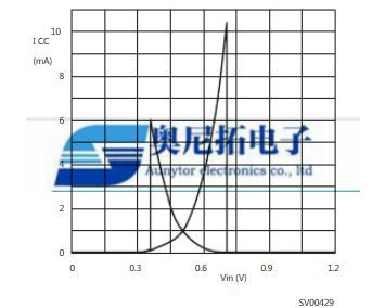
Typical 74LV14 transfer characteristics; V CC = 1.2V
Typical 74LV14 transfer characteristics; V CC = 2.0V
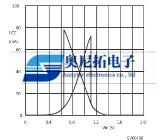
Typical 74LV14 transfer characteristics; V CC = 3.0V
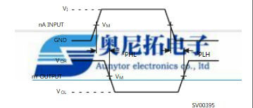
Input (nA) to output (nY) propagation delays
AC WAVEFORMS
VM= 1.5 V at V CC = 2.7 V;
VM= 0.5×V CC at V CC < 2.7 V
V OL and V OH are the typical output voltage
drop that occur with the output load
Part No Temp(℃) Package
74LV14N -40℃ to +125℃ SOT27
74LV14D -40℃ to +125℃ SOT108
74LV14DB -40℃ to +125℃ SOT337
74LV14PW -40℃ to +125℃ SOT402
FROM: Company Name: Aunytor Electronic (HK) Co.,Ltd
Contact Person: Charlotte
Skype: Aunytor
whatsapp:+86 13537622113
Email: carrot@aunytorchips.com