


Description
The SN74CBTLV3125 quadruple FET bus
switch features independent line switches.
Each switch is disabled when the associated
output-enable (OE\) input is high.
This device is fully specified for partial-
power-down applications using Ioff. The Ioff
feature ensures that damaging current will not
backflow through the device when it is powered
down. The device has isolation during power off.
To ensure the high-impedance state during power
up or power down, OE\ should be tied to VCC
through a pullup resistor; the minimum value
of the resistor is determined by the current-sinking
capability of the driver.
Features
Standard °Ø125-Type Pinout
5-¶∏ Switch Connection Between Two Ports
Rail-to-Rail Switching on Data I/O Ports
Ioff Supports Partial-Power-Down Mode Operation
Latch-Up Performance Exceeds 100 mA Per JESD 78, Class II
logic diagram (positive logic)
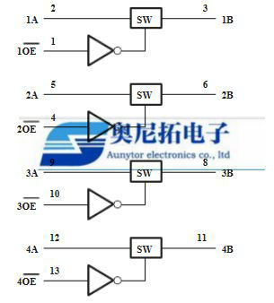
Pin numbers shown are for the D, DGV, NS, PW, and RGY packages
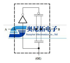
simplified schematic, each FET switch
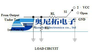
PARAMETER MEASUREMENT INFORMATION
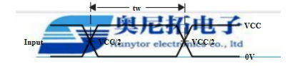
VOLTAGE WAVEFORMS PULSE DURATION
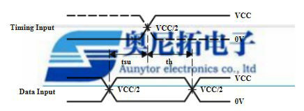
VOLTAGE WAVEFORMS SETUP AND HOLD TIMES
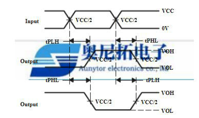
VOLTAGE WAVEFORMS PROPAGATION DELAY TIMES
INVERTING AND NONINVERTING OUTPUTS
VOLTAGE WAVEFORMS ENABLE AND DISABLE TIMES
LOW- AND HIGH-LEVEL ENABLING
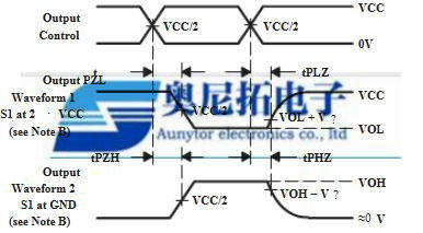
NOTES: A. CL includes probe and jig capacitance.
B. Waveform 1 is for an output with internal conditions such that the output is low except when disabled by the output control.
Waveform 2 is for an output with internal conditions such that the output is high except when disabled by the output control.
C. All input pulses are supplied by generators having the following characteristics: PRR =10 MHz, ZO = 50Ω,tr =2 ns, tf =2 ns.
D. The outputs are measured one at a time with one transition per measurement.
E. tPLZ and tPHZ are the same as tdis.
F. tPZL and tPZH are the same as ten.
G. tPLH and tPHL are the same as tpd.
H. All parameters and waveforms are not applicable to all devices
Part No Temp(°Ê) Package
74CBTLV3125DBQRE4 -40 to 85 SSOP (DBQ)-16
74CBTLV3125DBQRG4 -40 to 85 SSOP (DBQ)-16
74CBTLV3125PWRE4 -40 to 85 TSSOP (PW)-14
74CBTLV3125PWRG4 -40 to 85 TSSOP (PW)-14
SN74CBTLV3125D -40 to 85 SOIC (D)-14
SN74CBTLV3125DBQR -40 to 85 SSOP (DBQ)-16
SN74CBTLV3125DGVR -40 to 85 TVSOP (DGV)-14
SN74CBTLV3125DR -40 to 85 SOIC (D)-14
SN74CBTLV3125PW -40 to 85 TSSOP (PW)-14
SN74CBTLV3125PWG4 -40 to 85 TSSOP (PW)-14
SN74CBTLV3125PWR -40 to 85 TSSOP (PW)-14
SN74CBTLV3125RGYR -40 to 85 VQFN (RGY)-14
FROM: Company Name: Aunytor Electronic (HK) Co.,Ltd
Contact Person: liao
Skype: Aunytor
Email: 2885745253@qq.com