


Product Description:
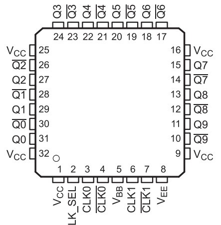
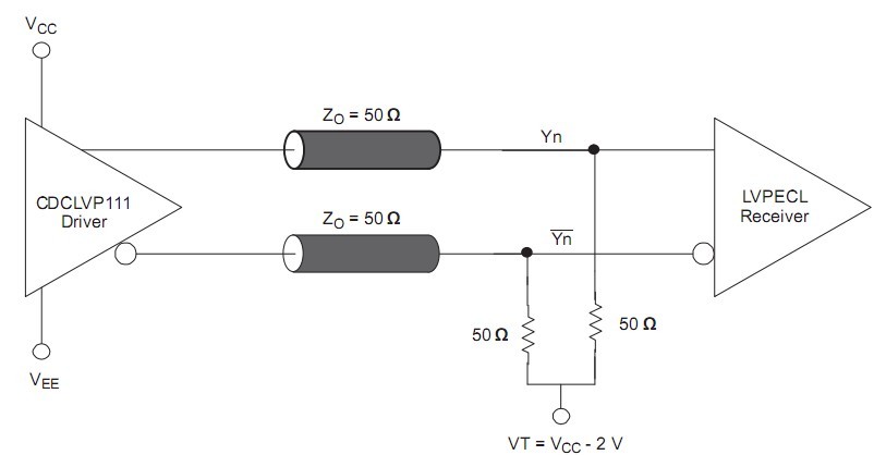
The CDCLVP111 clock drive is assigned a differential LVPECL clock input pair, (CLK0, CLK1) to 10 differential LVPECL clock (Q0, and nine parties) and the clock distribution outputs on the minimum offset. The CDCLVP111 can accept two clock sources into an input multiplexer. The CDCLVP111 is designed for driving 50 - transmission lines. When the output pins do not use, allow the proposal to reduce power consumption. If only one output pin from the use of differential pairs of the other output pins must be the same end 50.
In the VBB reference voltage output, if the use of single-ended input operation is necessary. In this case, VBB pin should be connected to the CLK0, with the GND 10 nF bypass capacitor.
However, high-speed performance up to 3.5 GHz, is the differential-mode is strongly recommended.
The CDCLVP111 is characterized by work in -40 °Ê to85 °„
Features:
Distribution of a differential LVPECL clock input pair and 10 differential LVPECL
Is fully compatible with LVECL / LVPECL signals
To support a wide supply voltage range from 2.375 V to 3.8 V
Optional clock input, through the CLK_SEL
Low output skew (15 ps typical value) clock distribution system
Additional jitter is less than 1 PS
Propagation delay of less than 350 ps of
Open Input Default State
LVDS, and leukemia, Surrey Satellite Technology is compatible with inputs
VBB reference voltage output for single-ended clock
32-pin LQFP and QFN packages
The frequency range from DC to 3.5 GHz
Pin-for-pin compatible with MC100 Series EP111, ES6111, LVEP111, PTN1111
Application:
Designed for driving 50 transmission lines
High-performance clock distribution
Specifications:
Status of the devices temperature (oC) Price (USD) | Quantity Package | pin to the top mark Package QTY | Package Carrier
CDCLVP111RHBR ACTIVE -40 to 85 5.55 | 1ku QFN (RHB) | 32 View 3000 | LARGE T & R
CDCLVP111RHBT ACTIVE -40 to 85 6.15 | 1ku QFN (RHB) | 32 View 250 | SMALL T & R
CDCLVP111VF ACTIVE -40 to 85 5.55 | 1ku LQFP (VF) | 32 View 250 | JEDEC TRAY (10 +1)
CDCLVP111VFR ACTIVE -40 to 85 5.55 | 1ku LQFP (VF) | 32 View 1000 | LARGE T & R
Product Diagram:
FROM: Company Name: Aunytor Electronic (HK) Co.,Ltd
Contact Person: liao
Skype: Aunytor
Email: 2885745253@qq.com
Contact Person: liao
Skype: Aunytor
Email: 2885745253@qq.com