

PDF AND WORD DOWNLOAD


AC-Coupled Hall-Effect Gear-Tooth Sensor ICs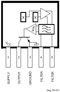
The A3059KA has been phased out of production as of October 31, 2005. For samples and information on the replacement part, please refer to the A1423LK.
The UGN/UGS3060KA has been phased out of production. For samples and information on the replacement part, please refer to the A1422LK.
Features
- Senses Motion of Ferrous Targets Such as Gears
- Wide Operating Temperature Range
- Operation to 30 kHz
- Resistant to RFI, EMI
- Large Effective Air Gap
- 4.5 V to 24 V Operation
- Output Compatible With All Logic Families
- Reverse Battery Protection
- Resistant to Physical Stress
Description
The UGS3059KA and UGN/UGS3060KA ac-coupled Hall-effect gear-tooth sensor ICs are monolithic integrated circuits that switch in response to changing differential magnetic fields created by moving ferrous targets. These devices are ideal for use in non-zero-speed, gear-tooth-based speed, position, and timing applications such as in anti-lock braking systems, transmissions, and crankshafts.
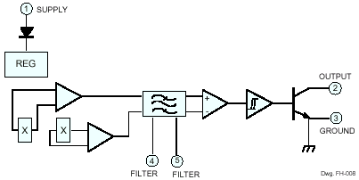
Both devices, when coupled with a back-biasing magnet, can be configured to turn ON or OFF with the leading or trailing edge of a gear-tooth or slot. Changes in fields on the magnet face caused by a moving ferrous mass are sensed by two integrated Hall transducers and are differentially amplified by on-chip electronics. This differential sensing design provides immunity to radial vibration within the devices' operating air gaps. Steady-state magnet and system offsets are eliminated using an on-chip differential band-pass filter. This filter also provides relative immunity to interference from RF and electromagnetic sources. The on-chip temperature compensation and Schmitt trigger circuitry minimizes shifts in effective working air gaps and switch points over temperature, allowing operation to low frequencies over a wide range of air gaps and temperatures.
Each Hall-effect digital Integrated circuit includes a voltage regulator, two quadratic Hall-effect sensing elements, temperature compensating circuitry, a low-level amplifier, band-pass filter, Schmitt trigger, and an open-collector output driver. The on-board regulator permits operation with supply voltages of 4.5 to 24 volts. The output stage can easily switch 20 mA over the full frequency response range of the sensor IC and is compatible with bipolar and MOS logic circuits.
Functional Block Diagram